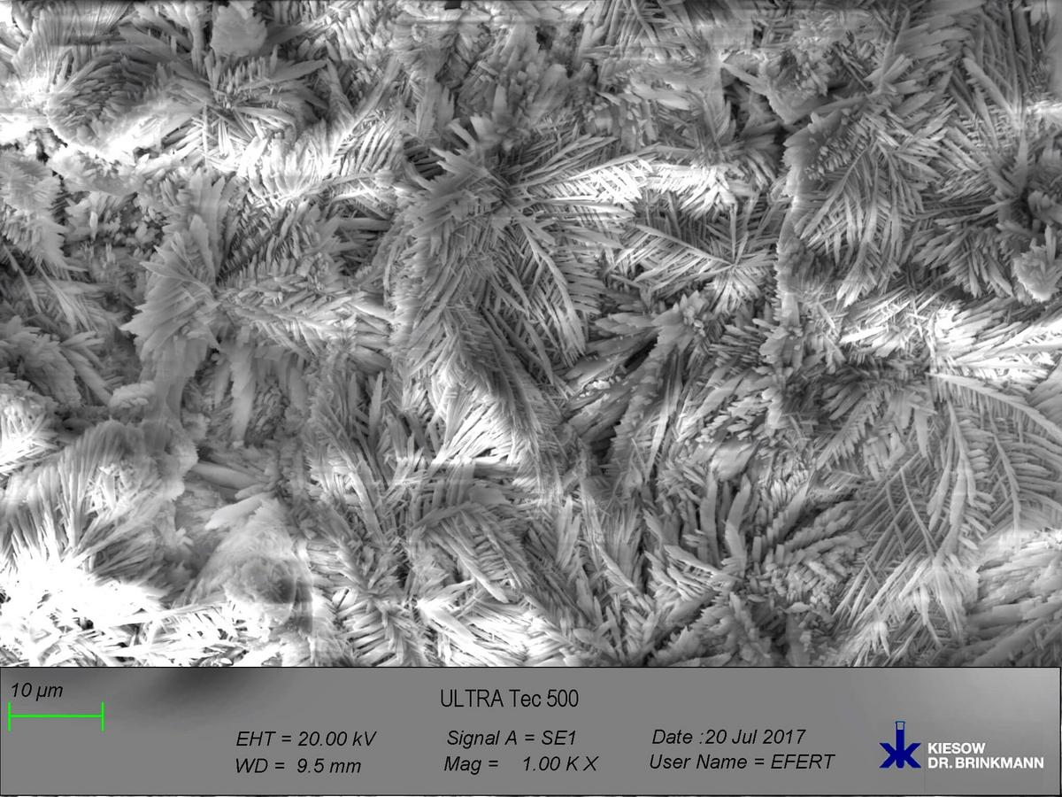
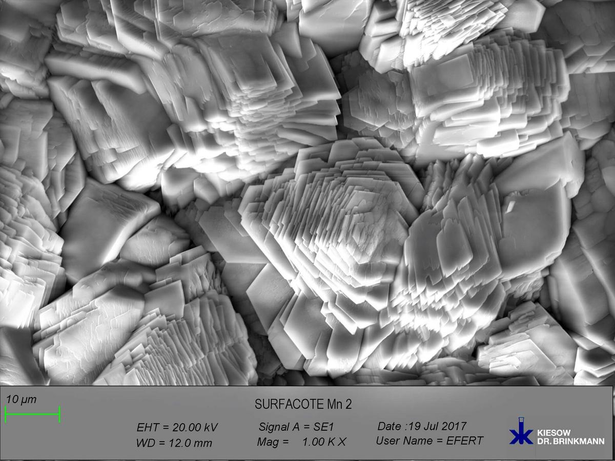
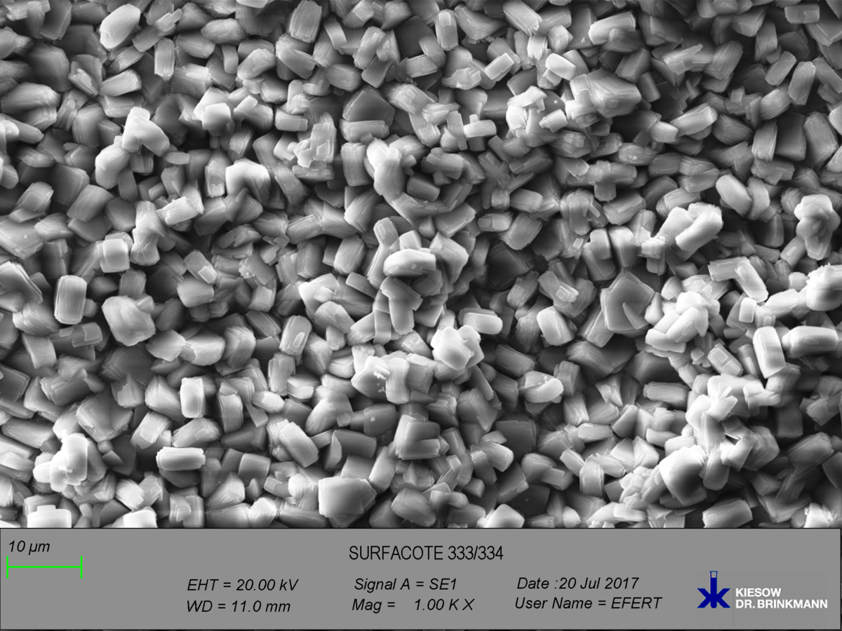
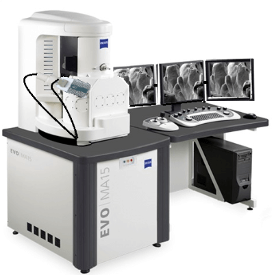
Scanning electron microscope
Research and development with assistenz of the scanning electron microscope.
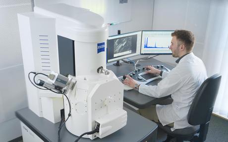
Cross sections and simple surface structures can be analyzed and photographed in our laboratory using a standard reflected-light microscope. However, microscope images with a high depth of field can no longer be visualized by using this conventional method. The scanning electron microscope provides a remedy at this point.
In contrast to the reflected-light microscope, the scanning electron microscope (SEM) enables images to be taken with high magnification and extremely high depth of field. We use this advantage specifically for the detailed representation and assessment of our produced surfaces, such as phosphatings, passivations and galvanic layers in the field of research and development.
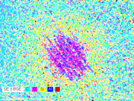
EDX analysis
In addition to excellent topographic imaging (SEM imaging), elemental analysis of conductive surfaces can be performed using EDX (energy dispersive X-ray analysis) to determine the chemical composition of the surface.
As a customer, are you interested in surface images?
We will be happy to send you a price quotation for this. Please fill out the contact form for this purpose.
Website:Contact form

